HISTORY OF RISC
Even before computers became as ubiquitous as they are now, they occupied a
place in students’ hearts and a place in engineering buildings, although it was
usually under the stairs or in the basement. Before the advent of the personal computer,
mainframes dominated the 1980s, with vendors like Amdahl, Honeywell,
Digital Equipment Corporation (DEC), and IBM fighting it out for top billing in
engineering circles. One need only stroll through the local museum these days for
a glimpse at the size of these machines. Despite all the circuitry and fans, at the
heart of these machines lay processor architectures that evolved from the need
for faster operations and better support for more complicated operating systems.
The DEC VAX series of minicomputers and superminis—not quite mainframes,
but larger than minicomputers—were quite popular, but like their contemporary
architectures, the IBM System/38, Motorola 68000, and the Intel iAPX-432, they
had processors that were growing more complicated and more difficult to design
efficiently. Teams of engineers would spend years trying to increase the processor’s
frequency (clock rate), add more complicated instructions, and increase the
amount of data that it could use. Designers are doing the same thing today, except
most modern systems also have to watch the amount of power consumed, especially
in embedded designs that might run on a single battery. Back then, power
wasn’t as much of an issue as it is now—you simply added larger fans and even
water to compensate for the extra heat!
The history of Reduced Instruction Set Computers (RISC) actually goes back
quite a few years in the annals of computing research. Arguably, some early work in
the field was done in the late 1960s and early 1970s by IBM, Control Data Corporation
and Data General. In 1981 and 1982, David Patterson and Carlo Séquin, both at the
University of California, Berkeley, investigated the possibility of building a processor
with fewer instructions (Patterson and Sequin 1982; Patterson and Ditzel 1980),
as did John Hennessy at Stanford (Hennessy et al. 1981) around the same time.
Their goal was to create a very simple architecture, one that broke with traditional
design techniques used in Complex Instruction Set Computers (CISCs), e.g., using
microcode (defined below) in the processor; using instructions that had different
4 ARM Assembly Language
lengths; supporting complex, multi-cycle instructions, etc. These new architectures
would produce a processor that had the following characteristics:
• All instructions executed in a single cycle. This was unusual in that many
instructions in processors of that time took multiple cycles. The trade-off
was that an instruction such as MUL (multiply) was available without having
to build it from shift/add operations, making it easier for a programmer,
but it was more complicated to design the hardware. Instructions in
mainframe machines were built from primitive operations internally, but
they were not necessarily faster than building the operation out of simpler
instructions. For example, the VAX processor actually had an instruction
called INDEX that would take longer than if you were to write the operation
in software out of simpler commands!
• All instructions were the same size and had a fixed format. The Motorola
68000 was a perfect example of a CISC, where the instructions themselves
were of varying length and capable of containing large constants along with
the actual operation. Some instructions were 2 bytes, some were 4 bytes.
Some were longer. This made it very difficult for a processor to decode the
instructions that got passed through it and ultimately executed.
• Instructions were very simple to decode. The register numbers needed for
an operation could be found in the same place within most instructions.
Having a small number of instructions also meant that fewer bits were
required to encode the operation.
• The processor contained no microcode. One of the factors that complicated
processor design was the use of microcode, which was a type of “software”
or commands within a processor that controlled the way data moved internally.
A simple instruction like MUL (multiply) could consist of dozens of
lines of microcode to make the processor fetch data from registers, move
this data through adders and logic, and then finally move the product into
the correct register or memory location. This type of design allowed fairly
complicated instructions to be created—a VAX instruction called POLY,
for example, would compute the value of an nth-degree polynomial for an
argument x, given the location of the coefficients in memory and a degree
n. While POLY performed the work of many instructions, it only appeared
as one instruction in the program code.
• It would be easier to validate these simpler machines. With each new generation
of processor, features were always added for performance, but that
only complicated the design. CISC architectures became very difficult to
debug and validate so that manufacturers could sell them with a high degree
of confidence that they worked as specified.
• The processor would access data from external memory with explicit
instructions—Load and Store. All other data operations, such as adds, subtracts,
and logical operations, used only registers on the processor. This differed
from CISC architectures where you were allowed to tell the processor
to fetch data from memory, do something to it, and then write it back to
An Overview of Computing Systems 5
memory using only a single instruction. This was convenient for the programmer,
and especially useful to compilers, but arduous for the processor
designer.
• For a typical application, the processor would execute more code. Program
size was expected to increase because complicated operations in older
architectures took more RISC instructions to complete the same task. In
simulations using small programs, for example, the code size for the first
Berkeley RISC architecture was around 30% larger than the code compiled
for a VAX 11/780. The novel idea of a RISC architecture was that
by making the operations simpler, you could increase the processor frequency
to compensate for the growth in the instruction count. Although
there were more instructions to execute, they could be completed more
quickly.
Turn the clock ahead 33 years, and these same ideas live on in most all modern
processor designs. But as with all commercial endeavors, there were good RISC
machines that never survived. Some of the more ephemeral designs included DEC’s
Alpha, which was regarded as cutting-edge in its time; the 29000 family from AMD;
and Motorola’s 88000 family, which never did well in industry despite being a fairly
powerful design. The acronym RISC has definitely evolved beyond its own moniker,
where the original idea of a Reduced Instruction Set, or removing complicated
instructions from a processor, has been buried underneath a mountain of new, albeit
useful instructions. And all manufacturers of RISC microprocessors are guilty of
doing this. More and more operations are added with each new generation of processor
to support the demanding algorithms used in modern equipment. This is referred
to as “feature creep” in the industry. So while most of the RISC characteristics found
in early processors are still around, one only has to compare the original Berkeley
RISC-1 instruction set (31 instructions) or the second ARM processor (46 operations)
with a modern ARM processor (several hundred instructions) to see that the
“R” in RISC is somewhat antiquated. With the introduction of Thumb-2, to be discussed
throughout the book, even the idea of a fixed-length instruction set has gone
out the window!
1.2.1 ARM Begins
The history of ARM Holdings PLC starts with a now-defunct company called
Acorn Computers, which produced desktop PCs for a number of years, primarily
adopted by the educational markets in the UK. A plan for the successor to the
popular BBC Micro, as it was known, included adding a second processor alongside
its 6502 microprocessor via an interface called the “Tube”. While developing an
entirely new machine, to be called the Acorn Business Computer, existing architectures
such as the Motorola 68000 were considered, but rather than continue to
use the 6502 microprocessor, it was decided that Acorn would design its own. Steve
Furber, who holds the position of ICL Professor of Computer Engineering at the
University of Manchester, and Sophie Wilson, who wrote the original instruction
6 ARM Assembly Language
set, began working within the Acorn design team in October 1983, with VLSI
Technology (bought later by Philips Semiconductor, now called NXP) as the silicon
partner who produced the first samples. The ARM1 arrived back from the fab
on April 26, 1985, using less than 25,000 transistors, which by today’s standards
would be fewer than the number found in a good integer multiplier. It’s worth noting
that the part worked the first time and executed code the day it arrived, which
in that time frame was quite extraordinary. Unless you’ve lived through the evolution
of computing, it’s also rather important to put another metric into context,
lest it be overlooked—processor speed. While today’s desktop processors routinely
run between 2 and 3.9 GHz in something like a 22 nanometer process, embedded
processors typically run anywhere from 50 MHz to about 1 GHz, partly for power
considerations. The original ARM1 was designed to run at 4 MHz (note that this is
three orders of magnitude slower) in a 3 micron process! Subsequent revisions to the
architecture produced the ARM2, as shown in Figure 1.3. While the processor still
had no caches (on-chip, localized memory) or memory management unit (MMU),
multiply and multiply-accumulate instructions were added to increase performance,
along with a coprocessor interface for use with an external floating-point accelerator.
More registers for handling interrupts were added to the architecture, and one
of the effective address types was actually removed. This microprocessor achieved
a typical clock speed of 12 MHz in a 2 micron process. Acorn used the device in
the new Archimedes desktop PC, and VLSI Technology sold the device (called the
VL86C010) as part of a processor chip set that also included a memory controller,
a video controller, and an I/O controller.
Registers
The register is the most fundamental storage area on the chip. You can put most
anything you like in one—data values, such as a timer value, a counter, or a coefficient
for an FIR filter; or addresses, such as the address of a list, a table, or a stack in
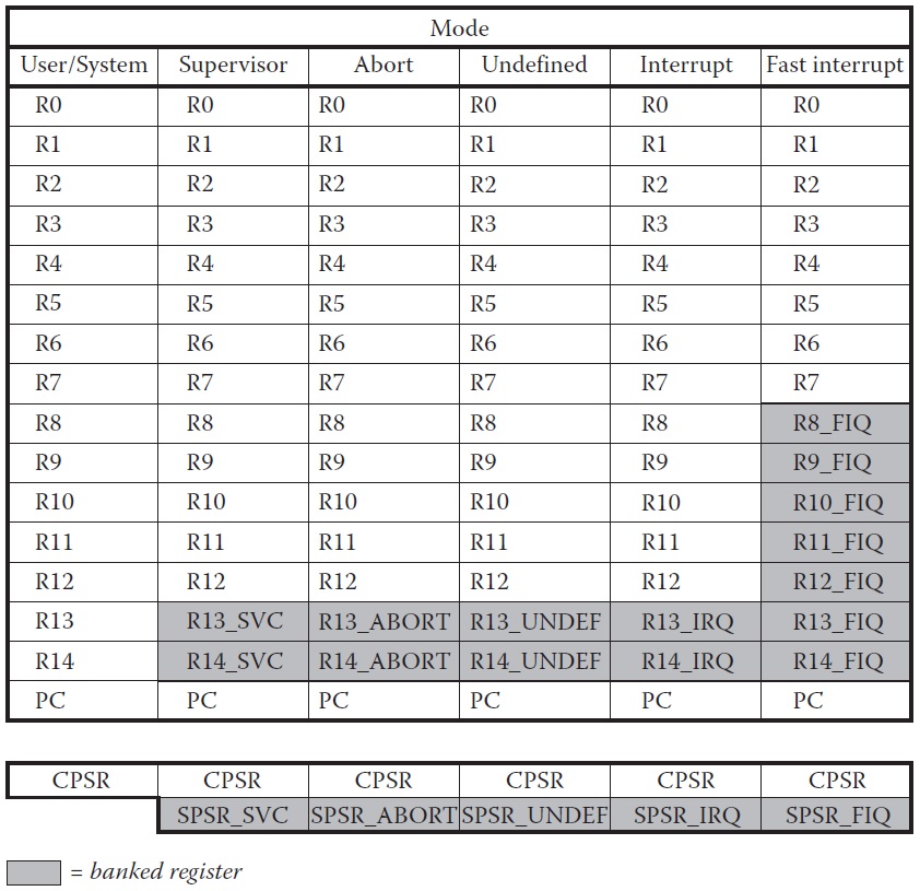
memory. Some registers are used for specific purposes. The ARM7TDMI processor
has a total of 37 registers, shown in Figure 2.2. They include
• 30 general-purpose registers, i.e., registers which can hold any value
• 6 status registers
• A Program Counter register
The general-purpose registers are 32 bits wide, and are named r0, r1, etc. The
registers are arranged in partially overlapping banks, meaning that you as a programmer
see a different register bank for each processor mode. This is a source of
confusion sometimes, but it shouldn’t be. At any one time, 15 general-purpose registers
(r0 to r14), one or two status registers, and the Program Counter (PC or r15) are
visible. You always call the registers the same thing, but depending on which mode
you are in, you are simply looking at different registers. Looking at Figure 2.2, you
36 ARM Assembly Language
can see that in User/System mode, you have registers r0 to r14, a Program Counter,
and a Current Program Status Register (CPSR) available to you. If the processor
were to suddenly change to Abort mode for whatever reason, it would swap, or bank
out, registers r13 and r14 with different r13 and r14 registers. Notice that the largest
number of registers swapped occurs when the processor changes to FIQ mode. The
reason becomes apparent when you consider what the processor is trying to do very
quickly: save the state of the machine. During an interrupt, it is normally necessary
to drop everything you’re doing and begin to work on one task: namely, saving the
state of the machine and transition to handling the interrupt code quickly. Rather
than moving data from all the registers on the processor to external memory, the
machine simply swaps certain registers with new ones to allow the programmer
access to fresh registers. This may seem a bit unusual until we come to the chapter
on exception handling. The banked registers are shaded in the diagram.
While most of the registers can be used for any purpose, there are a few registers
that are normally reserved for special uses. Register r13 (the stack pointer or SP)
holds the address of the stack in memory, and a unique stack pointer exists in each
mode (except System mode which shares the User mode stack pointer). We’ll examine
this register
to be continued
HOME PAGE